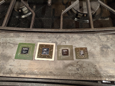
I based my procedure off of many YouTube videos I had seen on the subject. The idea is to use diamond lapping film to slowly sand off the shielding on the silicon dies to expose the surface beneath. I had all four of my victims ready to go:
From left to right, these are chips that came off of a NVIDIA Quadro FX 3450, an ATI Radeon 9800 Pro, a NVIDIA 8600GT, and a Radeon HD 2400 Pro. Instead of taking a blow torch to them, I decided to cook them on my stove through a thick piece of metal (that was really fun to quench in the sink). This separated the dies from the packages with a little bit of coaxing from my craft knife.
Once I separated the flipchip from the package, it was time to grind. I had to figure out a way to keep a steady and level hold over it. This is likely where I failed.
My bright idea was to take a large bolt and use it as a handle. To make it smooth, I lapped the surface, and then I added a square of adhesive strip to make it stick.
Take a good look at this Radeon HD 2400 Pro die, because it's the last time you'll see it in a good state.
This is my lapping station. I got a small pane of glass from the hardware store and the film from Amazon. I definitely could have done a better job assembling this, but I thought it would be good enough. This was likely my second mistake, but probably not as bad as the first or third mistake.
The third mistake was starting on too high of a grit. I thought I needed to dig through a layer of micro solder balls, remnant packaging, and a protective layer of silicon to get to the structures of the chips. This proved to be incorrect.
 |
| A larger chip before lapping |
So, what went wrong? The answer is obvious: uneven pressure. I also didn't know that the structures would be so shallow here, so I was blowing straight through the important layers in all the wrong places. Do I want to try this again? Yes. Will I do it soon? Probably not.


No comments:
Post a Comment